High-sensitivity elemental analysis using an analytical transmission electron microscope with Cs-corrector
In addition to functional devices such as electronic devices and energy devices, in the nanotech material field, the regions to be observed or analyzed are extremely minute. Therefore, at Sumika Chemical Analysis Service, we have introduced a TITAN 80-300 transmission electron microscope. This microscope is equipped with a spherical aberration correction mechanism (Cs collector) boasting world-class spatial resolution. We respond to analysis needs that are growing more sophisticated every year by making the most of cutting-edge evaluation equipment and know-how accumulated over many years.
Background
In development of advanced materials, control of the structure and composition of materials has reached the atomic level, and the high-resolution analytical electron microscope is an indispensable analytic tool.
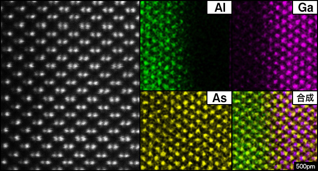
At Sumika Chemical Analysis Service, we can use an aberration-corrected analytical electron microscope, equipped with a high-sensitivity elemental analysis system, to not only conduct elemental analysis with high spatial resolution, but also elemental analysis with high speed and low damage by making using of high sensitivity.
Features
- High-sensitivity, high-precision composition analysis
The high-sensitivity elemental analysis system enables element analysis with high speed and low damage. - High-resolution STEM observation
Enables observation of quality, high-resolution STEM images by combining a spherical aberration correction system with a cold-field-emission electron gun (Cold-FEG) - Various types of special observation to suit the purpose of evaluation
We have environmental control, cooling, and a special-purpose holder for tasks such as 3D observation, and this enables diverse types of special observation and analysis.
Other Applications
| terms | overview |
|---|---|
| transmission electron microscope(TEM)image | This is an image formed by electrons transmitted through a sample (transmission electrons). It is created by elastically scattered electrons. There are two observation methods: the bright-field method and the dark-field method. |
| scanning transmission electron microscope(STEM)image | This image is obtained by scanning a thin sample with a microscopic electron probe. A disc-shaped detector measures the strength of transparent waves (or diffracted waves) from the sample, and this is displayed on a monitor synchronized with the probe scan. The resolution is determined by the diameter of the probe, and there are two observation methods: the bright-field method and the dark-field method. |
| dark-field image | Electron beams that are directly transmitted are blocked, so the image is formed only from electron beams that have scattered. A characteristic of dark-field images is that boundary lines (such as crystal grain boundaries or twin planes) show up clearly. |
| bright-field image | An image is formed of electron beams that transmit through the sample (without scattering or refracting). Therefore, refracted areas appear dark, while areas that are not refracted appear bright. Along with dark-field images, these images are used when measuring membrane thickness and analyzing lattice defects for samples. |
| spherical aberration | This is an aberration that creates a spherical and blurry image. This is caused when an electron beam passes through the edge of the lens, and instead of arriving on the optical axis of the ideal image field, it arrives at a location off from the optical axis (or slightly toward the front [of the lens] on an electron microscope). This is the most important of all aberrations in field lenses. |
| Cs corrector | A device that creates a negative spherical aberration coefficient to cancel the positive spherical aberration coefficient of lenses that are symmetrical to the magnetic field axis (field lenses and condenser lenses). The high TEM image resolution (caused by correcting the spherical aberration of the field lens) and the high resolution HAADF image (caused by correcting the spherical aberration of the condenser lens) make it possible to conduct element analysis from a single row of atoms. |
| electron diffraction | In this method, the sample is exposed to an electron beam to obtain information on the crystal structure from the obtained diffraction pattern. If the sample is a crystal, this method can be used to obtain information on the regularity of the atomic arrangement, the periodicity, the symmetry, and disarray from crystal lattice integrity. If the sample is non-crystalline, this method can be used to determine the distance of nearby atoms (first, second, and so on) and quantity. Electron beams can be set finer than X-ray beams, so it is possible to obtain the diffraction pattern from the local field. |
| energy-dispersive X-ray spectroscopy(EDS) | In this method, a sample is exposed to an electron beam. The X-ray energy generated from the sample is broken down into a spectrum, from which the chemical elements included in the sample can be analyzed. Although this cannot be used to analyze light chemical elements (boron [B] or lighter elements), it provides more efficient detection than wavelength dispersive X-ray spectroscopy. It also requires less exposure current than wavelength dispersive X-ray spectroscopy, so it is less damaging to the sample. |
| elastically scattered electron | These are electrons that scatter without losing energy when incident electrons collide with atoms and move in a different direction (scatter). If the sample is thin, the strength of the TEM image or diffraction pattern can be explained by elastically scattered electrons. If the sample is thick (10 nm), the effect of inelastically scattered electrons must be considered. |
| inelastically scattered electron | These are electrons that scatter after losing some energy when the incident electron interacts with electrons in the crystal or crystal lattices. Although the possibility of inelastic scattering occurring is at least one digit smaller than elastic scattering, if the sample is thick (10 nm or thicker), the contribution of inelastically scattered electrons will stack with elastic scattering, making the TEM image or electron diffraction pattern unclear. Transmission electron microscopes equipped with energy filters are used to eliminate inelastic scattering. |
| electron energy-loss spectroscopy(EELS) | In this method, the energy of inelastic scattering electrons generated by the interaction between incident electrons and the sample are dispersed, and then a quantitative/qualitative analysis or electron state analysis is performed on chemical elements in the micro region. |
| high-angle annular dark-field scanning transmission electron microscopy(HAADF-STEM) | In the scanning transmission electron microscope (STEM) method, a disc-shaped detector gathers electrons that undergo inelastic scattering at a high angle due to thermal diffuse scattering caused by lattice vibration. The resulting image shows the strength of these electrons. This method can even be used with substances that have no periodicity. The image strength is proportional to the square of the atomic number, allowing selective observation of heavy atoms. The resolution is determined by the size of the incident beam. The most powerful of these devices can be used together with EELS to analyze chemical elements of 0.1 nm or thinner at the atomic level. |
| tomography | In this method, a sample is continuously photographed at an angle to generate multiple projection images. These images are processed on a computer to recreate the internal structure of the sample in three dimensions. This method was developed from cross-sectional photography using X-ray CTs and MRIs in the medical field, then applied to TEM images. |
| lattice image | This image corresponds to a crystal lattice obtained by interfering with the transparent waves and diffracted waves from a thin and crystalline sample. Changes in the strength of the lattice image do not properly correspond with changes in the electrostatic potential of the sample photographed in the direction of the incident electron beam. However, it can be used to determine the periodic structure of crystals. |
| crystal orientation | This represents the direction of the crystal as a plane index of the crystal. When observing with a transmission electron microscope, the specific direction of the crystal (specifically, the direction indicated by the low-order index) is aligned with the direction of the incident electron beam. |
Technical News
Contact Us for Services
For inquiries and requests concerning services of analysis, measurements, products and consulting, please contact us via inquiry form.