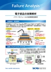
We’ll introduce the latest process assessment technologies for power semiconductors that carry out critical roles through controlling efficient electric energy.
Please click the "Request Document" button and register your information for document request.
Evaluation of Electronics & MEMS
NEWElectronic Part Failure Analysis
In order to realize high reliability of power modules, which are power semiconductor devices, we contribute by analyzing failure phenomena and elucidating the contributing factors using various analytical methodologies.
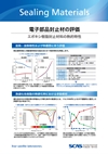
Electronic Part Sealant Assessment
We preform assessments of epoxy sealing resin for a property of thermophysics of heat dissipation. We assess thermal characteristics by combining thermal conductivity measurement with thermodilatometric measurement.
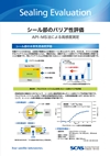
Seal Barrier Assessment
It is critical to assess in a highly sensitive manner both the functionality of barrier film that protects devices as well as the barrier capability of the seal area that adheres to the devices.
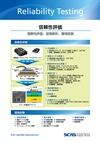
Reliability Assessment
Semiconductor devices, electronic parts, electronic materials, functional materials and the like can be checked for issues such as defects and failure through undergoing reliability testing.
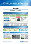
Environmental Testing
"We undertake environmental testing according to various testing standards.
Here we introduce a summary of composite salt spray cycle testing, chemica resistance testing, and corrosive gas testing."
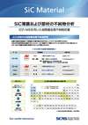
Evaluation of SiC
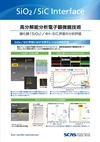
High Resolution Analysis Electronic Microscopic Technologies
For MOSFET devices post-annealing, structural analysis of SiO2/SiC interface and the atomic level are possible using the transmission electronic microscopes.
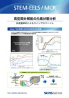
High Spatial Resolution Element Analysis
It is possible to analyze element states by EELS spectral multivariate analysis from the results of sub-nano level high spatial resolution via STEM with an onboard Cs corrector.
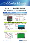
SiC Carrier Concentration Assessment and Stress Estimate
Visible laser irradiatin of chemical compound semiconductors with polarity such as SiC induces observation of Raman spectra with longitudinal and transverse waves originating from crystal lattice oscillation.
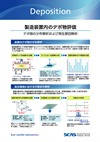
Manufacturing Device Deposit Assessment
Accurately assessing distribution of deposits on inner wall of manufacturing equipment enables accurate consideration of cleaning recipes, making it possible to connect cleaning to improvements in yield.
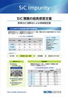
SiC Membranes and Material Impurity Analysis
Applying various pre-treatment methods enables analysis of metal impurities by ICP-MS in all processes from SiC substrate and epitaxial films to devices.
SiC Membrane Ultra High Sensitivity Quantification
The new pre-treatment methods make it possible to quantify metal impurities included in insoluble SiC material bulk, surface, and thin films by ppb orders with ICP-MS.
To request the Document
Please click the "Request Document" button and register your information for document request.
Contact Us for Services
For inquiries and requests concerning services of analysis, measurements, products and consulting, please contact us via inquiry form.