Manufacturing process temperatures of electronic devices using organic semiconductor materials are near room temperature, and suitable for manufacturing lightweight, flexible electronic devices based on plastic and paper substrates.
Now we’ll discuss the latest technologies for organic semiconductors and organic materials.
Please click the "Request Document" button and register your information for document request.
Devices Defects Analysis
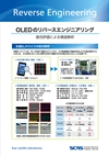
NEWReverse Engineering of OLED
OLED devices consist of many materials. In order to analyze its physical structure, constituent materials and defects, it is necessary to combine several methods according to the purpose.
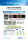
Strucral Analysis of OLED lighting devices.
LAADF-STEM is effective for cross-section observation of multilayer structure such as OLED Lithing. Thin film composition analysis is possible by combining high sensitivity element analysis.
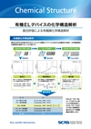
Analysis of Chemical Structures of OLED Devices
To analyze the chemical structure and layer structure of organic compounds in OLED devices, it is necessary to combine appropriate analytical methods.
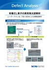
Analysis of abnormal light-emitting defects in OLED devices
Cross-Sectional Observation of the device structure by FIB-SEM and laser Raman method that can be measured in a sealed state is effective for analyzing the cause of the abnormal light-emitting defects generated in the OLED device.
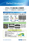
Analysis of Defect Analysis in Glass/ITO film.
The confocal laser microscope can detect and observe defects in transparent materials such as quartz wafers and ITO films. In addition, highly accurate defect marking technology and FIB-STEM-EDS enable detailed analysis of defects.
Process Contamination, Impurity Analysis
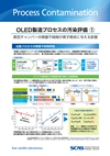
Reverse Engineering of OLED Manufacturing Process Contamination Analysis 1
The operational lifetime of an OLED device may change due to differences in vacuum chambers and fabrication time. In order to improve operating life it is important to analyze and manage process contamination.
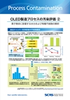
Reverse Engineering of OLED Manufacturing Process Contamination Analysis 2
This describes a case study of impurity analysis around the time of vacuum chamber cleaning as an example of checking whether water or organic impurities have an effect on element life.
The influence of water and organic impurities on the lifetime of the OLED device was analyzed for impurities in the vacuum chamber before and after cleaning.
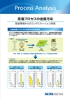
Metal Contamination in Vapor Deposition Process
Impurities contaminate the OLED device from material and fabricating environment. controlling the contamination status of the fabrication process is important for performance improvement and yield improvement.
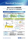
Residual Solvent in the Wet Process
Analysis of thermal desorption behavior of residual solvent by TG-MS and highly sensitive determination of residual solvent by DHS-GC-MS are effective for optimizing drying conditions in wet process.
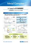
Ir(ppy)3 Impurity Analysis
The purity of the OLED material affects the characteristics and lifetime of the OLED device. Impurity analysis of materials is effective for improving the material purification process.
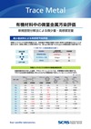
Analysis of Trace Metal Contamination in Organic Material
It is desirable that few samples are used for analysis. We can quantify trace metals with small amount of sample.
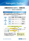
Analysis of Trace Halogen and Sulfur in Organic Material
Halogen and sulfur analysis can be quantified at the level of 0.X ppm with a small sample by blank control technology.
Materials, Thin Films
Analysis of Crystallization/Orientation in Organic Thin Films
In multilayer analysis of OLED devices, we propose analytical methods according to purpose.
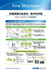
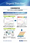
Analysis of Organic Thin Films
We introduce analysis examples of PAR-XPS as a method to evaluate the composition and orientation of the SAM in the depth direction.
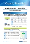
Analysis of Crystallization/Orientation in Organic Thin Films
We introduce XAS and GIXD using synchrotron radiation effective for analysis of crystallinity and orientation of organic thin films.
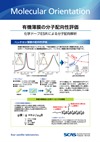
Analysis of Molecule Orientation in Organic Membrane
Pentacene forms a thin film with anisotropy. Chemical doping
ESR can evaluate anisotropy of pentacene thin film.
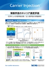
Analysis of Carrier Concentration in Thin Films Interface
The electron spin resonance method (ESR) can evaluate the amount of charge generated at the transport layer / injection layer interface in the state of a laminated film.
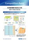
Analysis of Codeposition Thin Film Composition Ratio
The distribution of the dopant is possible by measuring the ratio of each compound in the co-evaporated film with high accuracy.
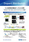
Phosphorescent Material Light Emission Dopant Distribution
MALDI - TOF / MS mapping is effective for dopant distribution analysis.
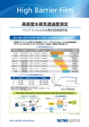
Highly-Sensitive Mesurement of Water Vaper Transmission Rate
API - MS compliant with ISO 15106 - 06 can evaluate water vapor transmission rate at 10 - 6 g / m 2 / day with high sensitivity and high accuracy.
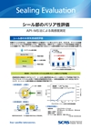
Barrier property analysis of adhesive part
In addition to evaluating the performance of the barrier film that protects the device, it is important to evaluate the barrier properties of the adhesive part that seals and bonds the structure.
To request the Document
Please click the "Request Document" button and register your information for document request.
Contact Us for Services
For inquiries and requests concerning services of analysis, measurements, products and consulting, please contact us via inquiry form.